

Pioneering Equipment Capabilities for Semiconductor Excellence

At Comptek, we provide state-of-the-art equipment powered by our proprietary Kontrox passivation technology, engineered to eliminate surface defects, enhance material quality, and optimize performance across semiconductor applications.
From scaling next-generation microLEDs to boosting laser efficiency and advancing power electronics, our high-performance tools are designed for precision, reliability, and seamless integration into your production workflows.
Complementing this is our in-depth characterization capability, ensuring that every process meets the highest industry standards of accuracy, quality and performance.
Explore our equipment capabilities and leverage Comptek's cutting-edge solutions to transform your semiconductor manufacturing.
TM
Scalability
From R&D to high-volume manufacturing, our equipment supports customers at every stage of their production journey.
Customization
Each tool is designed with flexibility in mind, allowing us to tailor processes to specific device architectures and applications.
Industry-Leading Quality
Built with premium components from trusted European manufacturers, our equipment guarantees exceptional reliability and performance.
Integrated Solutions
Seamlessly integrating Kontrox passivation with widely adopted industry methods, our equipment provides comprehensive solutions tailored to meet the advancing demands of next-gen semiconductor manufacturing.
How Comptek Equipment Powers Semiconductor Innovation?
Kontrox Wafer Processing Systems: From Lab to Pilot-Scale Production
TM

Kontrox 100mm Wafer Reactor
TM
Specialized for smaller wafer samples up to 100mm and R&D applications, this tool supports proof-of-concept development, process optimization, and material compatibility assessments. It enables customers to validate innovations efficiently, driving the advancement of cutting-edge technologies.
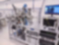
Kontrox 200mm Wafer Pilot Line Tool
TM
Tailored for larger wafers, this scalable R&D platform integrates Kontrox passivation with plasma-enhanced ALD to optimize surface quality and interfaces in III-V dielectrics and mesa structures. It reduces defects, enhances chip performance, and boosts yields for applications such as µLED sidewall passivation and gate stack dielectrics for power electronics.
Designed for seamless R&D-to-production transitions, this pilot-scale system enables manufacturers to scale next-gen device production with ease. Funded by the EIC "Enlight" project, it is a key driver of industrial-scale innovation in semiconductor manufacturing.

Key Features:
Automated cluster tool with high-vacuum connections for seamless integration between Kontrox™ reactor, ALD, and glove box
Designed for up to 200mm substrates, with storage for 10 wafers
Optimized for compound semiconductor processing in power electronics and optoelectronics
Flexible sample loading: works in ISO5 cleanroom, glove box, or atmospheric lab
In-situ monitoring for real-time surface characterization and process optimization on planar substrates
Configurations:
-
Base Pressure: 5*10 mbar
-
Process (wafer) temperature: up to 850°
-
Transfer speed between chambers: 30 sec
-
Sample holder options:: 200mm, 150mm, 100mm, 75mm, 50mm, 21 X 21mm, 20 x 20mm and 12mm x 12mm
-
Dimensions: 5.4 (w) X 4.0 (d) X 2.5m (h)
-10


Kontrox LASE 16: From Development to High-Volume Production
TM
Kontrox LASE 16 R&D Platform
TM
The Kontrox LASE 16 R&D Platform is a versatile process reactor that optimizes passivation processes for a wide range of applications, from edge-emitting lasers to smaller wafer samples. Engineered to support scalable, high-quality production, it enables manufacturers to validate innovations and achieve consistent, high-volume results.
Kontrox LASE 16 Industrial
TM
The fully automated Kontrox LASE 16 Industrial is our flagship commercial solution for high-volume edge-emitting laser facet passivation.
Featuring advanced cleaning, proprietary passivation, and optional precision sealing, this all-in-one system delivers premium quality at significantly lower costs. Its ability to produce highly stable passivated bars and streamline mirror coating empowers manufacturers to scale laser production with unmatched reliability, precision, and efficiency.

Characterization Equipment: Precision Analysis for Unmatched Results


Our comprehensive suite of characterization tools enables precise evaluation of material and device performance. Encompassing all phases of evaluation—from surface quality assessment to defect analysis—our specialized equipment ensures that every process step meets the highest industry standards.
With full-spectrum capabilities—from atomic-scale insights to device-level evaluation—we provide the detailed data needed to optimize production processes for maximum performance and efficiency.
Semiconductor Device & Material Analysis
-
LIV (Light-Intensity-Voltage) Measurements
-
C-V and Hg Probe C-V Mapper
-
Auger Electron Spectroscopy (AES)
-
SEM/EDX (Scanning Electron Microscopy / Energy Dispersive X-ray Spectroscopy)
-
FIB (Focused Ion Beam)
-
AFM (Atomic Force Microscopy)
-
Cathodoluminescence (CL)
-
Reflection High Energy Electron Diffraction (RHEED) & Low Energy Electron Diffraction (LEED)
-
Mass Spectrometry
-
UV-VIS Spectroscopy
-
At Partner Facility: SPM / HR-TEM, XPS
Advanced Proprietary Optical Data Acquisition and Analysis for Optoelectronic Devices
Multiscale TCAD Simulations
-
In-house developed MicroPL and TCSPC (carrier lifetime) with wavelength-resolved measurements for in-depth chip characterization.
-
Outstanding resolution and high-speed measurements
-
Full wafer or single pixel characterization
-
Classical drift-diffusion transport coupled with Poisson calculations
-
Multi-band EFA (Envelope Function Approximation) using k·p theory
-
Valence Force Field (VFF) module for atomistic structure relaxation
-
Atomistic Empirical Tight Binding (ETB) model for electronic structure analysis